Young Ceramics Networks
YCN Photo Contest 2017
Here are the results of the 2017 Photo Contest:
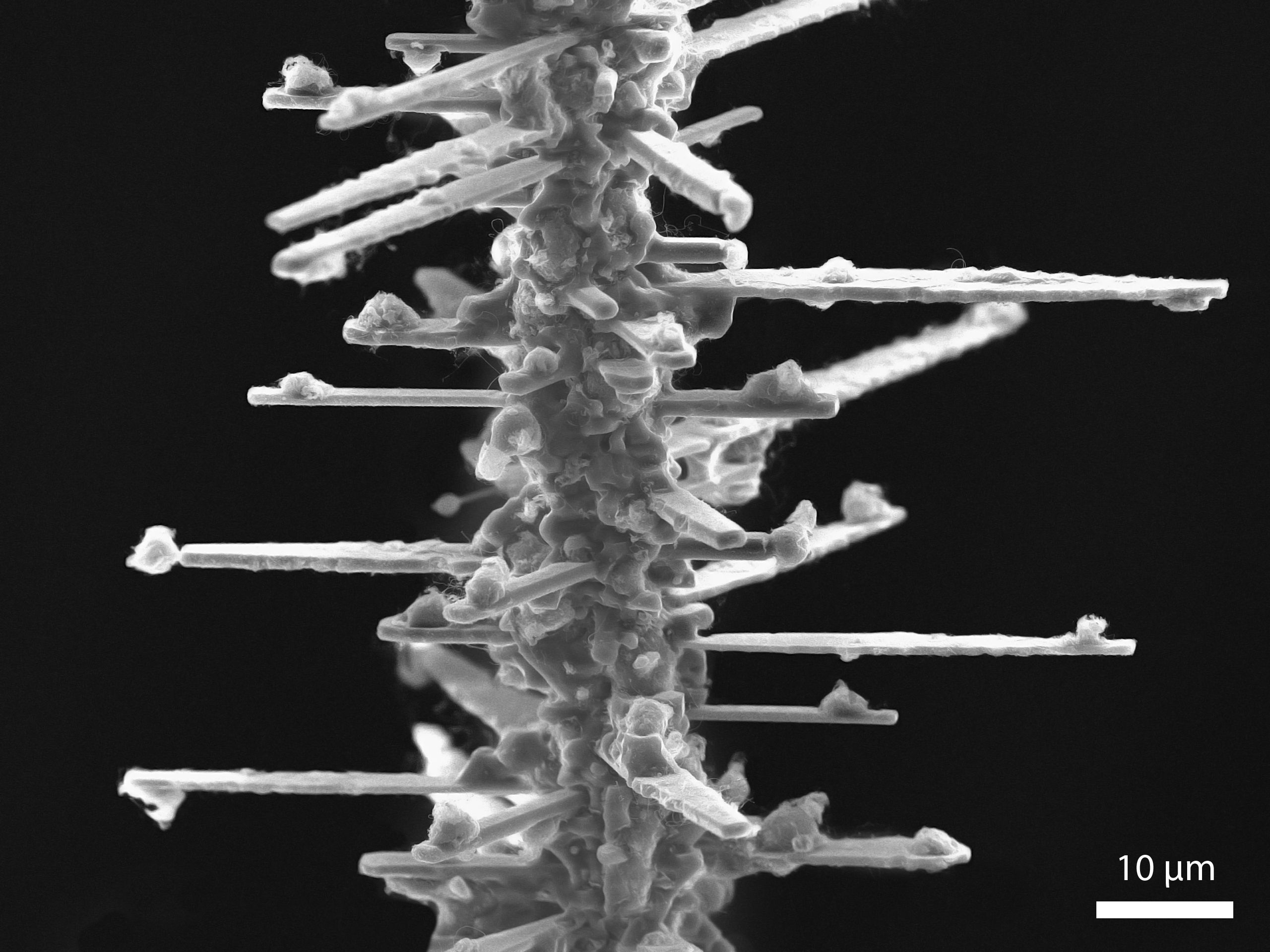
1. Ezra Feilden, Center for Advanced Structural Ceramics, Imperial College London, UK
Carbon Conifer
This structure was formed when growing a SiC layer on the surface of a carbon fiber. The original carbon fiber is the central structure, running from the bottom of the image to the top. SiC grows by precipitating liquid Si droplets on the fiber surface, which grow plates of SiC in a carbon rich atmosphere. These are the horizontal plates in the image, and the Si drops can still be seen at their tips. This process can also produce carbon nanotubes, which are the very small string-like structures seen across the surfaces.
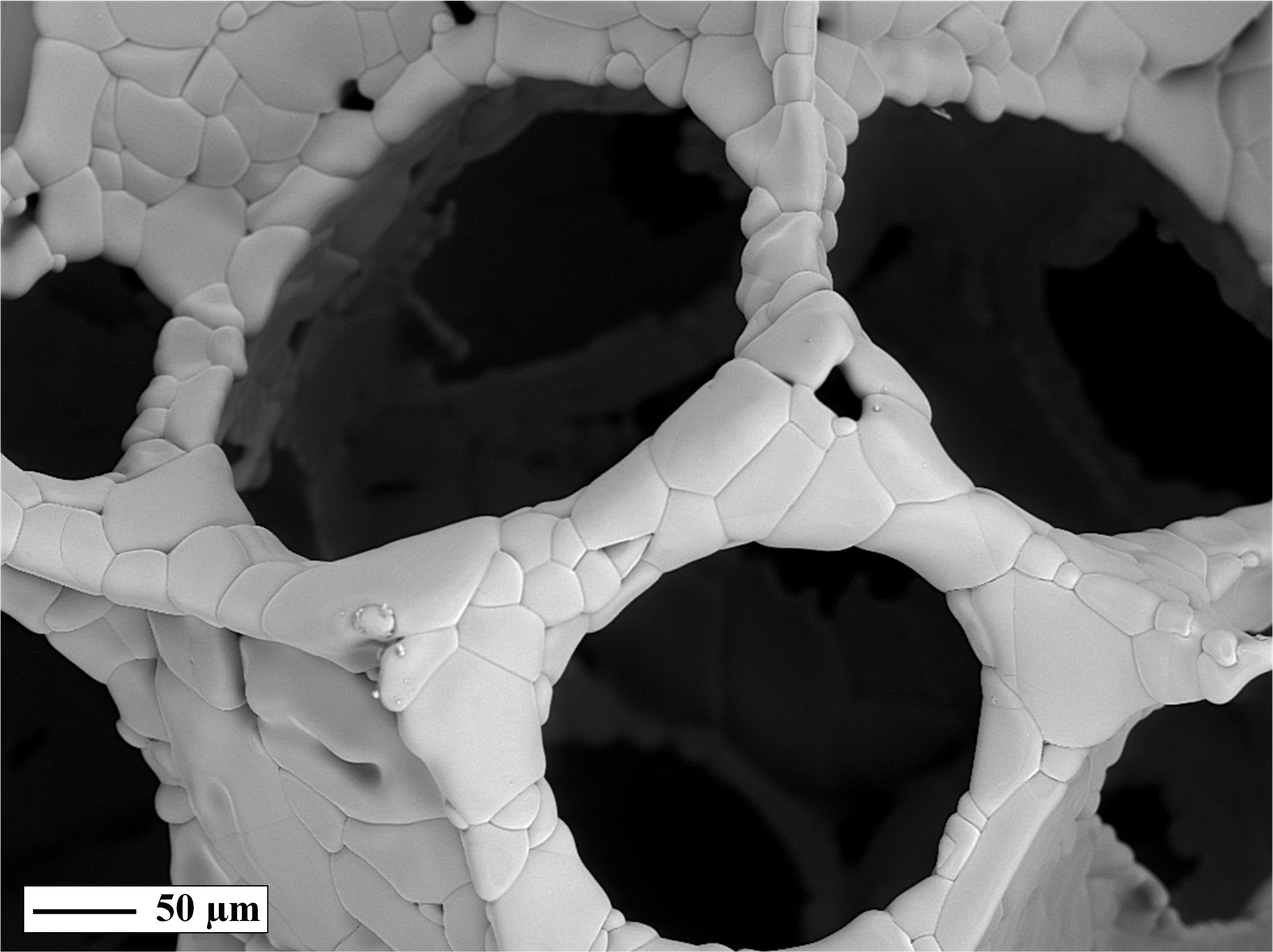
2. Līga Stīpniece, RTU Rudolfs Cimdins Riga Biomaterials Innovation and Development Centre, Institute of General Chemical Engineering, Latvia
Scream from the micron world
Highly porous titanium dioxide ceramic scaffolds obtained via polymer replica method for bone tissue regeneration
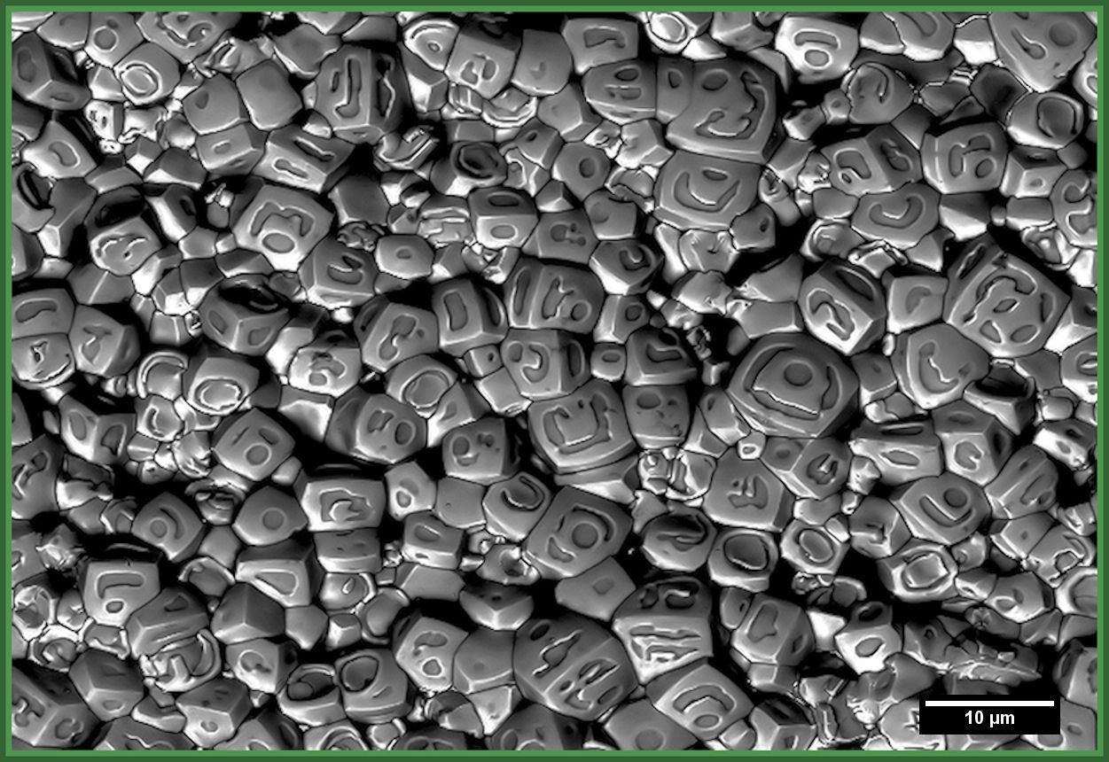
3. Ilkan Calisir, School of Materials, MSS Tower E16, The University of Manchester, M13 9PL, UK
Emojis in ceramics
"perovskite structured-lead-free ferroelectric ceramic"
Emojis have currently been an essential and a fun part of our daily communications via texting. However, it is not expected to see them at a sintered surface of ceramic with a few micron scales, under Scanning Electron Microscope, as appeared in the image. I investigate the core-shell type phase segregation in lead-free piezoceramics in my research and these unique features around the grains appeared as emoji-like have strengthened our proposal regarding to the formation mechanism that we have been thinking over for a long while. Eventually, the answer has been appeared as a smiley face.
Since the material seen here is one of the promising lead-free candidates among piezoceramics (mostly containing toxic lead), I also would like to emphasis on an issue that is vital for our world, which address the importance of research on environmentally-friendly materials represented as green border surrounding the image.
Image was taken by Scanning Electron Microscopy (Philips XL30 FEGSEM) under backscattered mode with 10 kV of accelerating voltage in the Electron Microscopy Centre, School of Materials, University of Manchester, United Kingdom.
Last news
YCN Newsletter 32 - Expert opinion - Maria Paula da Silva Seabra - CICECO, University of Aveiro
Turning Waste into Raw Materials for the Ceramic Industry.
Waste materials were once seen as a burden but are increasingly being redefined as valuable resources for ceramic production. Through advances in materials engineering, waste can be used as secondary raw materials in the ceramic industry. This shift enables more circular and resource-efficient ceramic manufacturing systems.
YCN Newsletter 32 - Industry in Spot - Dr. Daniel Bomze - Lithoz
Implementing 3D-Printed Technical Ceramics in Regulated Medical Fields.
Bringing a new manufacturing technology into medicine requires far more than producing an impressive component. In highly regulated fields, innovation must be translated into repeatable processes, documented quality, reliable materials and, ultimately, evidence of clinical value. Lithoz has spent more than a decade building this bridge for Lithography-based Ceramic Manufacturing (LCM).
Information
Contact us for any information: youngceramists@ecers.org - We will respond to your inquiry as soon as possible!


ECerS office
Av. Gouverneur Cornez , 4
7000 Mons
Belgium