
Young Ceramists Network
Welcome to our platform !
The nr.1 network in ceramics
Young Ceramists Network offers you all the benefits of networking in the world wide ceramics community.
Stay in touch with good friends and be the first to learn about new opportunities and events!
Montón Alejandro
SpainDefense University Centre Zaragoza

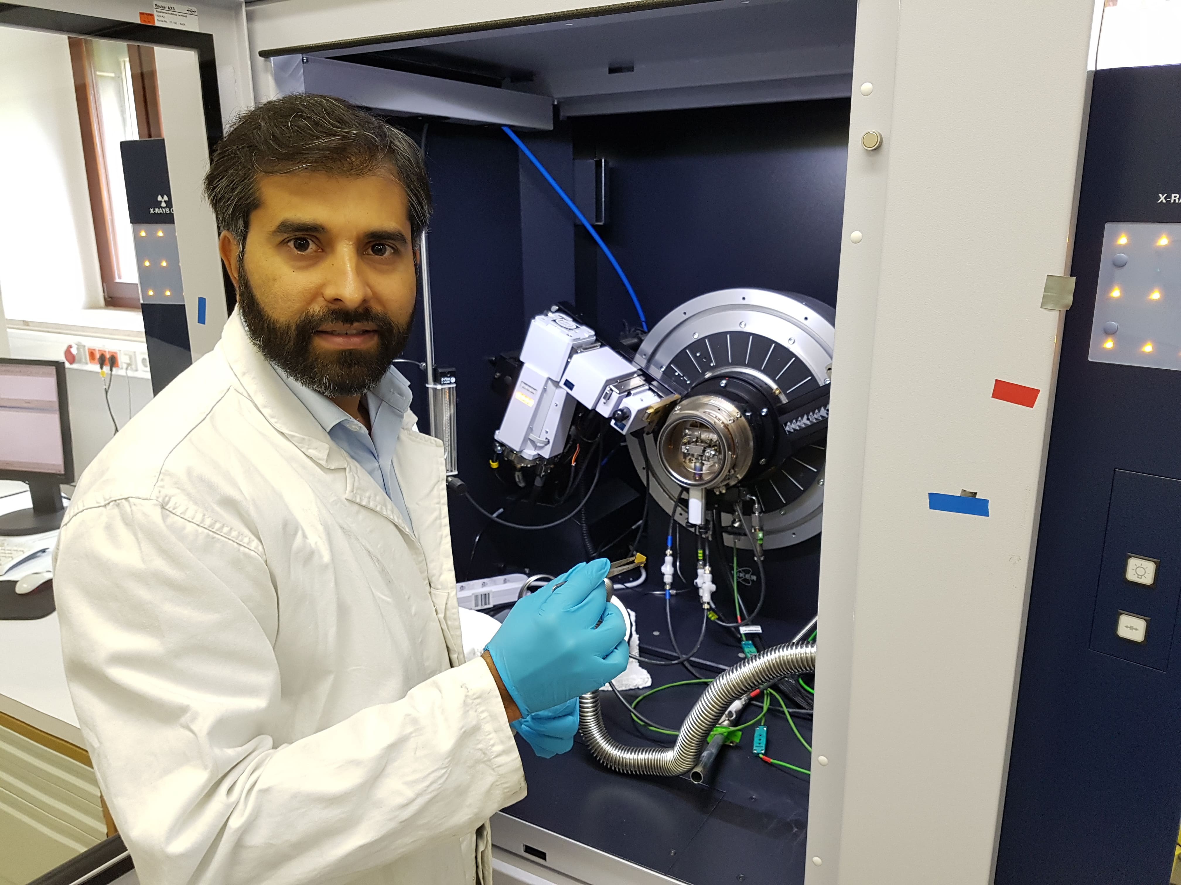
Qadir Awais
GermanyTU Bergakademie Freiberg
Huart Véronique
BelgiumEuropean Ceramic Society (ECerS)
Belot Aurore
BelgiumEuropean Ceramic Society (ECerS)

Frankberg Erkka J.
FinlandTampere University
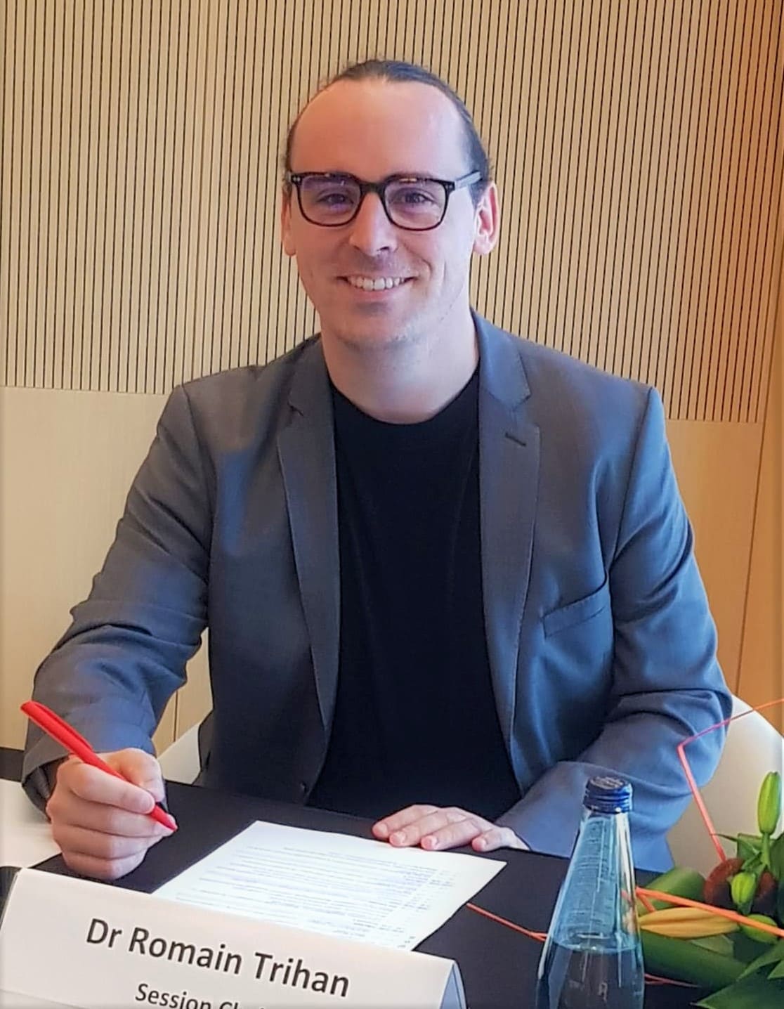
Trihan Romain
SwitzerlandEmpa
Abdelmoula Mohamed
EgyptAssiut University
Jabr Abdullah
AustriaMontanuniversitaet Leoben
Wahl Larissa
GermanyFriedrich-Alexander-Universität Erlangen-Nürnberg

Valášek Daniel
Czech RepublicCEITEC BUT
Tanska Joanna
PolandWarsaw University of Technology

Kocijan Martina
CroatiaUniversity of Rijeka

Chernomorets Dariia
UkraineInstitute for Single Crystals of the National Academy of Sciences
Ribeiro Camila
PortugalCICECO - Aveiro Institute of Materials, University of Aveiro
Kumar Muthusundar
BelgiumUniversity of Mons, Belgium

Salari Farid
The NetherlandsCONCR3DE Printing B.V.
Mota Morais Mateus
BrasilUniversity of Sao Paulo
Kirchner Katelyn
USACelSian Inc, Toledo OH

Nidžović Emilija
SerbiaCEXTREME LAB

Graboś Adrian
JapanTohoku University
Goričan Ivana
SloveniaJožef Stefan Institute

MOUNAJ Meryem
FranceCERAMATHS/DMP, Campus Universitaire de Maubeuge

Ojalvo Guiberteau Cristina
SpainGrupo Especializado de Materiales (GEMA)

Kovrlija Ilijana
LatviaInstitute of Biomaterials and Bioengineering, Faculty of Natural Sciences and Technology, Riga Technical University
Joksović Sara
SerbiaBioSense, Research and Development Institute for IT in biosystems

De la Torre Olvera Guido Manuel
SlovakiaCentre for Advanced Materials Application (CEMEA), Slovak Academy of Sciences, Dúbravská cesta 5807/9 845 11 Bratislava Slovakia


Conferences calendar
06/27 - XX ECerS Conference - Valencia 2027
The XXth Conference and Exhibition of the European Ceramic Society will take place from 27th June to 1st July 2027 in Valencia, Spain
09/26 - Shaping 10 Conference
The 10th Shaping conference will be organised by ECerS and the University of Padova from 21st to 23rd September 2026 in Padova, Italy.
10/26 - ElectroCeramics XX
The XXth ElectroCeramics Conference will be organised by ECerS and the University of Novi Sad from 12th to 15th October 2026 at the University of Novi Sad in Serbia.
Last news
YCN Newsletter 32 - Expert opinion - Maria Paula da Silva Seabra - CICECO, University of Aveiro
Turning Waste into Raw Materials for the Ceramic Industry.
Waste materials were once seen as a burden but are increasingly being redefined as valuable resources for ceramic production. Through advances in materials engineering, waste can be used as secondary raw materials in the ceramic industry. This shift enables more circular and resource-efficient ceramic manufacturing systems.
YCN Newsletter 32 - Industry in Spot - Dr. Daniel Bomze - Lithoz
Implementing 3D-Printed Technical Ceramics in Regulated Medical Fields.
Bringing a new manufacturing technology into medicine requires far more than producing an impressive component. In highly regulated fields, innovation must be translated into repeatable processes, documented quality, reliable materials and, ultimately, evidence of clinical value. Lithoz has spent more than a decade building this bridge for Lithography-based Ceramic Manufacturing (LCM).


ECerS office
Av. Gouverneur Cornez , 4
7000 Mons
Belgium